Chiplets Explained: How Modular Chips Build More Powerful Processors

For decades, a new processor often meant placing more capability onto one larger piece of silicon. Processing cores, cache, memory controllers, graphics, and input-output functions could all live together on a single die.
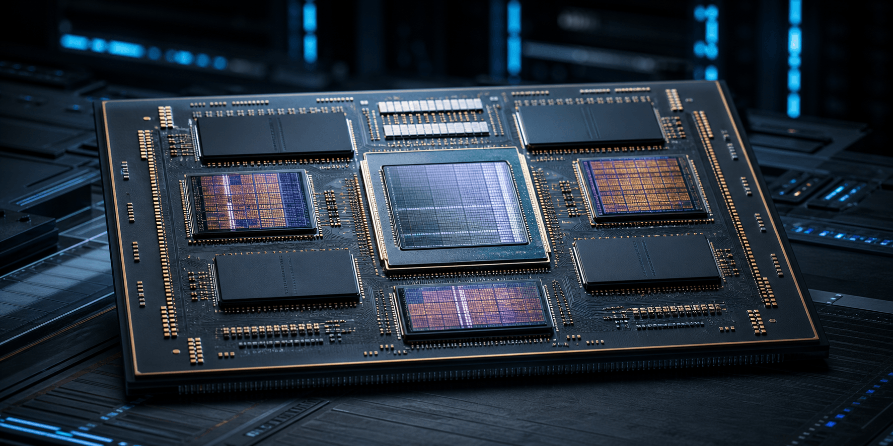
That monolithic approach is still useful. But as advanced chips become larger and more specialized, designers increasingly divide the work among several smaller dies called chiplets. Advanced packaging and fast die-to-die connections make them behave like parts of one processor.
Chiplets can improve manufacturing, reuse, and specialization. They also add communication, testing, thermal, and packaging challenges that a single die does not face.
What is a chiplet?
A chiplet is a small integrated circuit designed to perform part of a larger system's job. One might contain CPU cores, while others manage memory, external connections, graphics, cache, networking, security, or AI acceleration.
Three related terms help make the structure clear:
- A die is an individual piece of silicon cut from a manufactured wafer.
- A chiplet is a die intended to work as a modular part of a larger packaged system.
- A package holds and connects the dies, protects them, and helps move power, signals, and heat.
Chiplets are not normally components a consumer can swap. Their interfaces, timing, power, firmware, and layout are planned as part of the processor design.
How several dies become one processor
A chiplet system depends on its package as much as on its silicon. The package becomes a high-speed communication platform, not just a protective shell.
The design is divided by function
Engineers decide which functions belong together. Frequently communicating logic may need to remain close, while cutting-edge compute cores and mature input-output circuits may be better separated. Every boundary introduces another interface, so more pieces are not automatically better.
Each die is manufactured and tested
Each die can use the manufacturing process best suited to its work. Compute logic may benefit from a newer, denser process, while analog circuits and input-output functions may work well on a proven mature process. Testing before assembly identifies known-good dies so defective silicon is not combined with working parts.
Advanced packaging connects the pieces
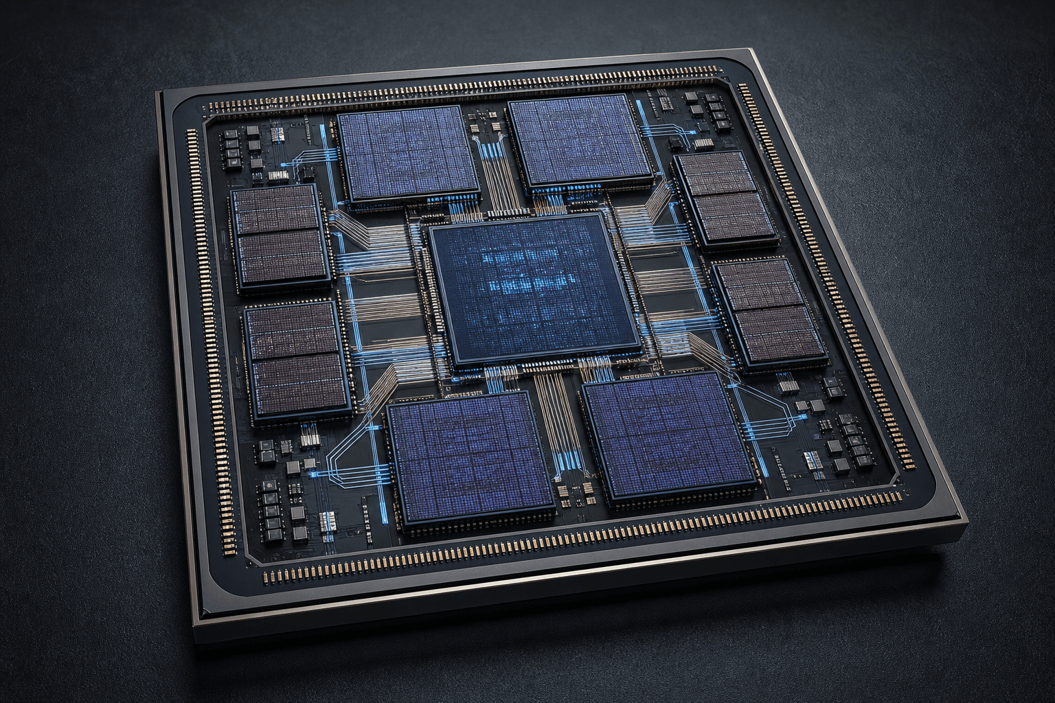
Chiplets can sit side by side on a package substrate, communicate across a silicon bridge or interposer, or be stacked vertically. These layouts are often described as 2D, 2.5D, and 3D integration.
Side-by-side placement can simplify cooling. An interposer or embedded bridge can support many short, dense connections. Vertical stacking can shorten some paths and increase density, but it makes heat removal and power delivery harder.
An interconnect carries data and control signals
The dies need a fast interconnect for data, memory requests, synchronization, errors, and power-management commands. The system may also need to keep caches and memory views consistent. A fast compute chiplet cannot help if it spends too much time waiting for another die.
Why designers use chiplets
Chiplets are not automatically faster than monolithic designs. Their main advantage is architectural freedom.
Smaller dies can improve manufacturing economics
A wafer contains many repeated dies, and a defect can make an affected die unusable. On the same manufacturing process, a smaller die generally has a better chance of avoiding a defect than a much larger one. That can improve component yield and reduce discarded silicon.
The final package still has its own yield: every die, connection, and assembly step must work. Chiplets move some manufacturing risk rather than eliminating it.
Different functions can use different processes
Shrinking every circuit onto the newest manufacturing node is not equally valuable. A chiplet design can place performance-sensitive logic on an advanced process and keep other functions on mature processes. Combining dies with different roles or technologies is called heterogeneous integration.
Proven blocks can be reused
A company can build a processor family around common blocks. The same input-output die might support several products while the compute chiplets change, reducing duplicated engineering across different performance and cost targets.
That modularity resembles the flexibility of cloud computing, where systems scale by combining resources rather than relying on one enormous machine. The physical engineering is very different, but both approaches benefit from components with clear responsibilities and dependable connections.
Specialized engines can sit close together
Modern workloads mix general processing with graphics, media, networking, encryption, and machine learning. A chiplet architecture can combine specialized engines without forcing every function into one giant design.
The fundamentals of machine learning involve repeated mathematical operations and large data flows. Specialized compute and nearby high-bandwidth memory can help, provided the package supplies enough bandwidth and removes the resulting heat.
The tradeoffs inside the package
Breaking a processor apart solves some problems by creating new ones.
Data movement costs time and energy
Signals crossing a die-to-die link generally face more distance and interface overhead than signals moving within one block. Poorly placed boundaries can add latency and power use. Architects respond by keeping closely coupled functions together, adding cache, widening links, or placing dies more densely.
Packaging becomes part of performance
Advanced substrates, bridges, interposers, and vertical connections require precise manufacturing. The package must deliver clean power, route high-speed signals, and maintain reliable connections. A die may pass alone yet fail after assembly because of a damaged connection, timing issue, or package defect.
Heat can become harder to remove
Several active dies can create uneven hot spots. Vertical stacking may place one heat-producing layer farther from the cooling surface, so floor planning, power limits, package materials, and cooling must work together.
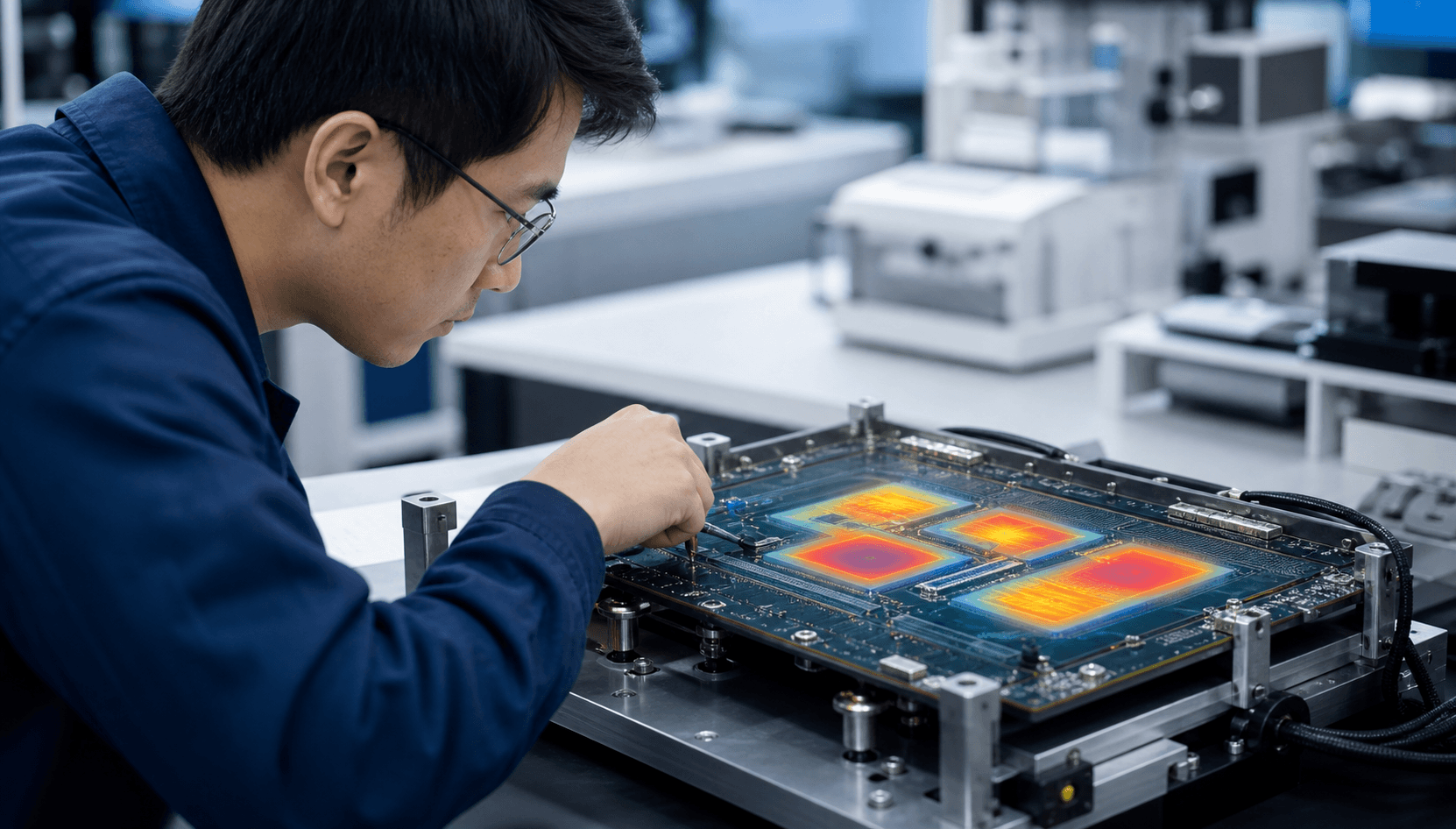
Power and thermal limits are especially important for compact devices. On-device AI places useful machine learning closer to the user, but local hardware still has to balance performance against battery life and heat. Chiplets offer more design choices; they do not repeal those physical constraints.
Verification spans more boundaries
Engineers must verify every die, the links, package, firmware, memory behavior, power states, and error handling. Security also crosses chiplet boundaries, requiring secure startup, controlled debugging, and a plan for faults in one component affecting the rest.
Why standards matter
Many chiplet products use connections designed for one company's components. The larger ambition is an ecosystem in which compatible dies from different teams or vendors combine more easily. The Universal Chiplet Interconnect Express standard, or UCIe, defines a common die-to-die connection framework for that goal.
A physical and protocol standard is necessary, but it is not the whole solution. Designers still need compatible package dimensions, power delivery, thermal limits, security models, firmware, test methods, and business agreements. The chiplet market is therefore not yet a simple catalog of interchangeable silicon parts.
Where chiplets make the most sense
Chiplets are attractive when a design needs large amounts of compute, several specialized functions, or a family of related products. Data-center processors can add compute dies, AI accelerators can combine compute with nearby memory, and networking or industrial systems can pair general processing with specialized acceleration.
The same idea can extend toward edge computing, where hardware must match the needs of factories, vehicles, communications equipment, and remote sites. Modular silicon may help designers create more targeted systems without rebuilding every block from the beginning.
For smaller products, one die may offer shorter connections, simpler packaging, and easier thermal behavior. The best architecture depends on volume, die size, workload, manufacturing options, and cost.
How to read chiplet claims
When a processor is described as chiplet-based, ask what the design actually gains:
- Which functions are separated into chiplets?
- Are the dies made on different manufacturing processes?
- How are they arranged and connected inside the package?
- What bandwidth, latency, and power costs come with those links?
- How are memory and cache kept coherent?
- How are dies tested before and after assembly?
- How does the package manage heat and power?
- Is the design truly interoperable, or are its chiplets specific to one product family?
The number of dies matters less than whether they divide the work sensibly and communicate efficiently.
The bottom line
Chiplets turn a processor into a modular system within one package. Smaller dies can improve manufacturing yield, use suitable process technologies, support reusable designs, and bring specialized compute close to memory and input-output.
The tradeoff is that packaging, interconnects, testing, heat, power, software, and security all become more complex. Communication between chiplets can cost more than communication within one die, and a defective connection can undermine otherwise working silicon.
Chiplets are not the end of monolithic processors or a shortcut around semiconductor physics. They are a powerful way to choose where complexity belongs. As packaging and interconnects improve, that choice will shape more personal devices, cloud systems, AI infrastructure, and edge machines.